Leading Chipmakers Aim to Make New Fabs More Sustainable
The recovering global economy is waking up to the notion that it now runs on silicon. And there isn’t enough of it.
Governments throughout the world are placing urgency on alleviating shortages of various types of chips. The semiconductor industry is talking about major capacity expansions across the industry—at a scope not seen in many years. Hundreds of billions of dollars have already been pledged to build new fabs around the globe.
The next generation of fabs will be distinguished by more than feature sizes. More than ever before, leading chipmakers are viewing the fab design task through the lens of sustainability.
At Applied Materials, we look forward to supporting this sustainability-minded capacity expansion. We know that chips enable applications like smart cities and electric vehicles that benefit the environment. Since chipmaking fabs consume a lot of energy and can churn out wafers for decades, why not use technology to add intelligence to the chipmaking process itself in order to reduce energy, water and chemical consumption and decrease carbon emissions?
In this blog, I look at ways to improve the efficiency of the sub-fab, the often-overlooked world of support equipment below the production floor that consumes around half of the energy needed by modern fabs. It’s a sea of pipes and pumps, ducts and heat exchangers, gas delivery and abatement systems that enable all of the high-tech equipment and chipmaking processes in the cleanroom above.
Sizing the Potential for Reductions
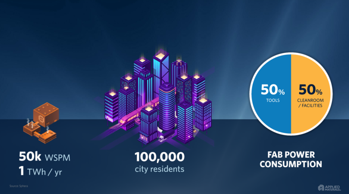
During a keynote at SEMICON West 2020, Applied’s CEO Gary Dickerson invited industry consultant Dr. Sarah Boyd to scope out the chipmaking sustainability challenge and opportunity for the industry. Dr. Boyd said over 1,000 fabs operate globally today, together producing over $500 billion worth of chips and about 50 million metric tons of CO2 each year. An advanced fab with a capacity of 50,000 wafer starts per month consumes roughly a terawatt-hour of electricity per year, close to what’s consumed by a city of 100,000 residents—like Santa Clara, California where Applied is headquartered. While half of the power is consumed by the wafer processing equipment, the other half is needed to power the support facilities and cleanroom (see Figure 1).
In other words, the machinery in the sub-fab contributes heavily to the power consumption and the related emissions. As the industry expands capacity, these support systems are prime targets for innovative solutions that can reduce the fab’s overall carbon footprint.
That’s where iSystem™ comes in.
Harvesting Data for Intelligent Control
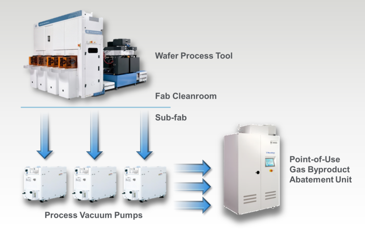
The more we can use technology to intelligently integrate the tools on the production floor with the sub-fab equipment, the more energy we can save (see Figure 2). iSystem is a software framework and network of controllers that gather data from both the tools and the sub-fab equipment so intelligent decisions can be made about operations and energy use.
In the past, sub-fab equipment operated at full power, even when production tools were idle such as during scheduled maintenance. iSystem vastly improves communications between tools and support systems, allowing engineers to modulate power with precision. Chipmaking is a delicate business, and you need data to intelligently calibrate the use of vacuum pumps and process gas abatement systems to avoid production disruptions and safety risks. iSystem monitors each tool’s operations and needs, safely dialing in the most energy-efficient settings.
A Leading Customer Delivers Impressive Results
TSMC recently published a case study about its work with Applied Materials and other suppliers to implement iSystem at its Fab 15B in Taichung City, Taiwan. The resulting solution saves 13.4 million kilowatt hours of electricity annually while reducing carbon emissions by 13,800 tons. iSystem is also being adopted in TSMC’s Fab 18 this year and is expected to be adopted across all of the customer’s 300mm fabs in Taiwan over time.
TSMC has a stated goal of achieving carbon neutrality and net zero emissions. The customer estimates these efforts will save 82 million kWh of electric energy annually, or 84.6 thousand tons of carbon emissions, generating energy saving benefits of NT$520 million ($18.6 million) in the future. These goals and savings are important steps in improving the carbon profile of the entire chipmaking industry.
The Future: More Data and AI
iSystem is currently connected to more than 3,000 tools across the industry, yet in many ways we are just at the beginning of what can be done to improve fab efficiency. Applied is working with semiconductor makers everywhere to understand and help achieve their sustainability goals. Through collaboration, we can use the power of Big Data and AI throughout all stages of semiconductor manufacturing.
In the next blog in this series, we will look at the production tools themselves and how Applied is working to reduce their energy usage, chemical consumption and cleanroom space requirements. Over time, we plan to enable a more holistic view of fab sustainability by combining energy data from the process tools and the sub-fab into a single report that process engineers can take action on. By working together with our customers and suppliers, we can help bring more new fabs online without adding to climate challenges.


